The Pritzker School of Molecular Engineering at the University of Chicago, under the direction of Giulia Galli, has published a computational analysis that forecasts the circumstances necessary to produce certain spin defects in silicon carbide. Their research, which was published online in Nature Communications, is a significant step forward in pinpointing manufacturing variables for spin defects that are beneficial for quantum technology.

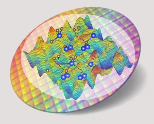
By using sophisticated computer simulations at the atomic scale, a new study predicts the formation process of spin defects useful for quantum technologies. Image Credit: Image by Emmanuel Gygi. With permission, a component of the figure is adapted from Christoph Dellago and Peter G. Bolhuis, Adv. Poly. Sci., Springer (2008)
Applications for quantum information, sensing, and communication benefit greatly from the abundance of electronic spin defects in semiconductors and insulators. Impurities and/or misplaced atoms are known as defects in a solid, and the electrons linked to these atomic defects have a spin. The fundamental unit of action in quantum technologies, the controlled qubit, could be created using this quantum mechanical feature.
However, the synthesis of these spin defects, which is normally accomplished experimentally through implantation and annealing procedures, is not well understood and, more critically, cannot be properly optimized. Different investigations have provided varied recommendations and outcomes for producing the appropriate spin defects in silicon carbide, an appealing host material for spin qubits due to its industrial availability.
There has not yet been a clear strategy to engineer the formation of spin defects to the exact specifications we want, a capability that would be highly advantageous for advancing quantum technologies. So, we embarked in a long computational journey to ask the following question: Can we understand how these defects form by carrying out comprehensive atomistic simulations?
Giulia Galli, Study Corresponding Author and Liew Family Professor, Molecular Engineering and Chemistry, University of Chicago
Galli’s team, which included Cunzhi Zhang, a postdoctoral researcher in Galli’s group, and Francois Gygi, a computer science professor at the University of California, Davis, paired multiple computational techniques and algorithms to predict the formation of specific spin defects known as “divacancies” in silicon carbide.
Divacancies are created by removing a silicon and a carbon atom sitting close together in a silicon carbide solid. We know from previous experiments that these types of defects are promising platforms for sensing applications.
Cunzhi Zhang, Postdoctoral Researcher, University of Chicago
Beyond what current technology can do, quantum sensing might detect magnetic and electric forces as well as explain how complicated chemical processes occur.
Galli added, “To unlock quantum sensing capabilities in the solid-state, we first need to be able to create the right spin defects or qubits at the right location.”
Galli and her colleagues utilized different ways to look at the motions of atoms and charges when a defect arises as a function of temperature to discover a formula for forecasting the generation of certain spin defects.
Typically, when a spin defect is created, other defects also appear and those may negatively interfere with the targeted sensing capabilities of the spin defect.
Francois Gygi, Professor, Computer Science, University of California, Davis
The first-principles molecular dynamics code Qbox, which is utilized in the team's quantum simulations, was mainly developed by Gygi.
“Being able to fully understand the complex mechanism of defect formation is very important,” Gygi noted.
The group combined the Qbox code with other cutting-edge sampling methods created at the Midwest Integrated Center for Computational Materials (MICCoM), a computational materials science center with its headquarters at Argonne National Laboratory and Department of Energy funding. Galli and Gygi are both senior investigators at MICCoM.
Galli stated, “Our combined techniques and multiple simulations revealed to us the specific conditions under which divacancy spin defects can be efficiently and controllably formed in silicon carbide. In our calculations, we are letting the fundamental physics equations tell us what is happening inside the crystal structure when defects form.”
The team warns, however, that generalizing their tool to predict a wider range of defect formation processes and defect arrays will require more work. The team anticipates that experimentalists will be interested in employing their computational tools to design a variety of spin defects in silicon carbide and also other semiconductors.
“But the proof of principle we have provided is important—we showed that we can computationally determine some of the conditions required to create the desired spin defects,” Galli further added.
Her team will then carry on with its efforts to broaden the computational research and accelerate the algorithms. Additionally, they want to broaden the scope of their investigation to cover a number of more plausible scenarios.
Galli added, “Here, we are only looking at samples in their bulk form, but in experimental samples there are surfaces, strain, and also macroscopic defects. We would like to include their presence in our future simulations and in particular understand how surfaces influence spin defect formation.”
All of her team’s predictions, according to Galli, are based on ongoing partnerships with experimentalists, even if her team’s advancement is based on computational investigations.
She concluded, “Without the ecosystem we work in, constantly talking with and partnering with experimentalists, this wouldn’t have happened.”
The Department of Energy is funding the research through the MICCoM (https://miccom-center.uchicago.edu/) and Q-NEXT (https://q-next.org/) centers.
Journal Reference
Zhang, C., et al. (2023) Engineering the formation of spin-defects from first principles. Nature Communications. doi:10.1038/s41467-023-41632-9