Reviewed by Alex SmithAug 13 2021
A non-destructive mechanism has been found by scientists from the University of Vienna’s Faculty of Physics to control donor impurities in silicon, achieved through focused electron irradiation.
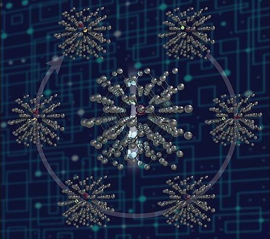
 Indirect exchange mechanism for the electron-beam manipulation of bismuth or antimony dopants in silicon based on computer simulations. The crimson sphere is a bismuth atom, while yellow and green spheres are respectively its nearest and next-nearest silicon neighbors. Image Credit: Toma Susi and Alexander Markevich / University of Vienna, Andrew R. Lupini.
This was performed in association with collaborators from the Oak Ridge National Laboratory in the United States.
As part of the latest indirect exchange process, there is not one but two neighboring silicon atoms involved in a coordinated atomic “waltz.” This might pave the way for the development of solid-state qubits. The study outcomes have been reported in the Journal of Physical Chemistry.
The ultimate aim of nanotechnology is to design materials at the atomic scale. Familiar examples of atom manipulation with scanning tunneling microscopy vary from the fabrication of quantum corals to rewritable atomic memories.
Yet, while fixed scanning probe methods are considered as potential tools for controlling surface atoms, it becomes hard for them to reach the bulk of the material as a result of the necessity to bring a physical tip into contact with the sample, generally requiring operation and storage at cryogenic temperatures.
The latest developments made in scanning transmission electron microscopy (STEM) have kindled the interest in the use of an electron beam for atom manipulation, and Vienna has emerged as one of the principal hubs of this study throughout the world.
The unique strength of this technique is its ability to access not only surface atoms but also impurities within thin bulk crystals. This is not only a theoretical possibility: the first proof-of-principle manipulation of bismuth dopants in silicon was recently demonstrated by our US collaborators.
Toma Susi, Faculty of Physics, University of Vienna
The latest collaborative work is a systematic modeling study on the electron-beam manipulation of group V dopant elements in silicon. Significantly, a new type of mechanism known as the indirect exchange was unraveled by the Vienna team.
This mechanism involves not just one but two neighboring silicon atoms in a coordinated atomic “waltz,” which describes the way in which electron effects could move such impurities inside the bulk of the silicon lattice.
While this mechanism only works for the two heavier donor elements, bismuth and antimony, it was crucial to find that it is non-destructive, as no atoms need to be removed from the lattice.
Alexander Markevich, Faculty of Physics, University of Vienna
As additional experimental progress, the team was able to show that it is possible to manipulate antimony impurities in silicon with the help of STEM. The accurate positioning of dopant atoms inside crystal lattices could allow novel applications in areas such as solid-state sensing and quantum computation. This might exhibit interesting implications.
Very recently, antimony dopants in silicon were suggested as promising candidates for solid-state nuclear spin qubits, and our work may open a path for their deterministic fabrication.
Toma Susi, Faculty of Physics, University of Vienna
The Vienna team was financially supported by the European Research Council (ERC) under the European Union’s Horizon 2020 research and innovation program (Grant agreement No. 756277-ATMEN), and the Oak Ridge National Laboratory group by the U.S. Department of Energy, Office of Science, Basic Energy Sciences, Division of Materials Sciences and Engineering as well as by the ORNL Laboratory Directed Research and Development Program.
Journal Reference:
Markevich, A., et al. (2021) Mechanism of Electron-Beam Manipulation of Single-Dopant Atoms in Silicon. Journal of Physical Chemistry C. doi.org/10.1021/acs.jpcc.1c03549.