Feb 12 2020
Photonic integration is an area of photonics that involves fabricating waveguides and devices onto a flat wafer to form an integrated system. This field is comparatively younger than electronics.
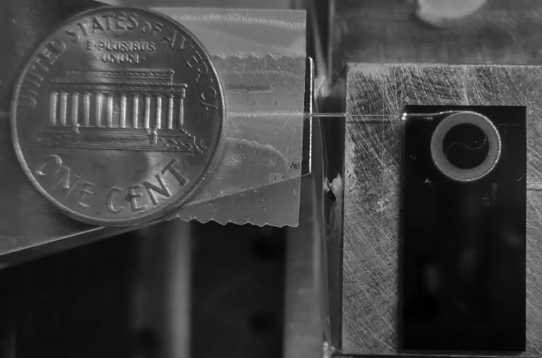
 A photonic integrated circuit in which an ultralow loss 2-meter optical waveguide guiding visible light in the red spectrum is put on a silicon nitride chip smaller than a penny, important for applications such as strontium atomic clocks. Image Credit: Nitesh Chauhan and the DARPA MTO ApHI program.
The focus of photonic integration has been on communications applications conventionally developed on silicon chips, as these are less costly and can be manufactured more easily.
Scientists have been studying potential new waveguide platforms that offer these same advantages for applications that run in the ultraviolet to the infrared spectrum. These platforms facilitate a considerably wider range of applications, such as precision metrology, spectroscopy for chemical sensing, and computation.
A paper published in APL Photonics, from AIP Publishing, offers an outlook of the area of ultra-wideband photonic waveguide platforms that are based on semiconductors with a wide bandgap. These integrated circuits and waveguides can achieve compact, power-efficient solutions, and can also transfer important portions of ultra-high-performance systems to the chip scale rather than huge tabletop instruments within a laboratory.
So far, important components and subsystems for applications like quantum communications, high-resolution spectroscopy, and atomic clocks are built on tabletops and in racks. This has been essential because they work at wavelengths that cannot be accessed by silicon waveguides because of its lower bandgap as well as other absorption properties in the UV to near-IR that restrict the optical power handling abilities, as well as other factors.
Daniel J. Blumenthal and his colleagues in Santa Barbara, California, have explored photonic integration platforms based on waveguides that are developed using semiconductors with wide bandgaps and ultralow propagation losses.
Now that the silicon market has been addressed for telecommunications and LIDAR applications, we are exploring new materials that support an exciting variety of new applications at wavelengths not accessible to silicon waveguides. We found the most promising waveguide platforms to be silicon nitride, tantala (tantalum pentoxide), aluminum nitride and alumina (aluminum oxide).
Daniel J. Blumenthal, Researcher, Santa Barbara, California
Each platform exhibits the capability to handle various applications, for example, aluminum oxide for UV interactions with atoms to enable quantum computing, tantalum pentoxide for Raman spectroscopy, or silicon nitride for atomic transitions in visible to near-IR.
Applications like futuristic high-capacity data center interconnects and atomic clocks in satellites can also take advantage of integrating functions like ultralow linewidth lasers onto low-power, lightweight chips. This is an area of higher focus as burgeoning data center capacity thrusts conventional fiber interconnects to their space and power restrictions.
According to Blumenthal, next-generation photonic integration will necessitate ultra-wideband photonic circuit platforms with the ability to scale from the UV to the IR, as well as provide a rich set of linear and nonlinear circuit functions, with ultralow loss and high-power handling abilities.