Jan 30 2020
At the U.S. Naval Research Laboratory, researchers have identified a novel platform for quantum technologies. They achieved this by suspending two-dimensional (2D) crystals over pores in a slab made of gold.
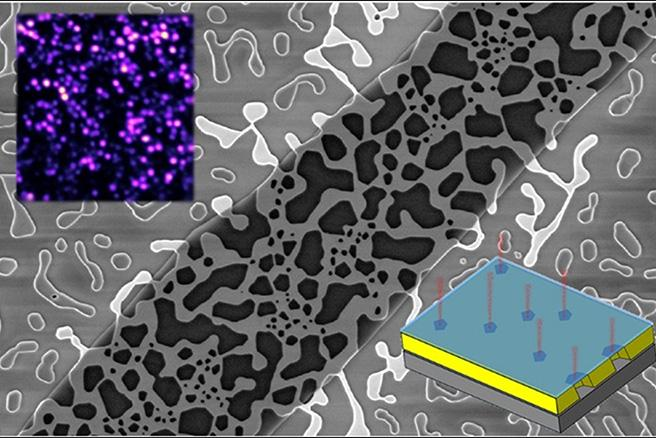
 Suspended two-dimensional crystals over pores in a slab of gold (center image) allow NRL scientists to connect quantum light sources (inset images) in a ready-made network. Image Credit: Jeremy Robinson/U.S. Naval Research Laboratory.
This new technique could help create new materials for sensing technologies and secure communication, based on the distinctive laws of physics at the atomic levels.
We never expected these atomically thin materials could influence the ordering of all of the atoms in such a relatively large slab of gold. When heated, the metal reflows to form a porous structure and the gold atoms lock into registry with the atoms in the 2D layer on top.
Jeremy Robinson, Materials Research Scientist, U.S. Naval Research Laboratory
The scientists anticipated they could see dewetting, a process caused by the interaction between surfaces of two solids. Rather than the formation of droplets on the glass base beneath the gold, due to heating, the underlying metal slab was reoriented. The gold turned porous throughout, and this physical change led the scientists to check for other side effects of the fusion.
We also discovered this combination can create a large number of quantum light sources in a, sort of, ready-made network. The alignment between atomic layers may facilitate energy transfer between the emitters through the gold framework that connects them.
Andrew Yeats, Research Physicist, U.S. Naval Research Laboratory
The light emitted from the 2D semiconductors was tested to find out whether it comes out as single light particles, or photons. These emitters have the ability to transfer energy to each other via the gold layer.
“We shine light on one part of the sample and we look at the light coming off at another part,” stated Robinson. “This teaches us how energy can be coupled into the gold layer at one point, propagated to a different quantum emitter site far away and re-emitted as light that we could see.”
Thanks to the potential to remotely control the transfer of energy to a single-photon emitter, this system proves to be appealing for quantum technology.
As we get better at controlling how the 2D semiconductor interacts with pores in the metal film, it’s easy to imagine different technologies that could use these properties. Sensors are a good first target, which can take advantage of the atomically thin membranes stretched across the porous metal framework.
Jeremy Robinson, Materials Research Scientist, U.S. Naval Research Laboratory
Although a gold slab was used by the team underneath the thin semiconductor layer to perform this study, other metals also have the ability to respond very similar to gold. Investigations are ongoing by the NRL team on how different material combinations and structures can form single-photon sources with exclusive properties, which is an important prerequisite for secure communications.