Mar 8 2019
A research team headed by the Department of Energy’s Lawrence Berkeley National Laboratory (Berkeley Lab) has devised a straightforward technique that could transform normal semiconducting materials into quantum devices—superthin devices characterized by exceptional electronic behavior.
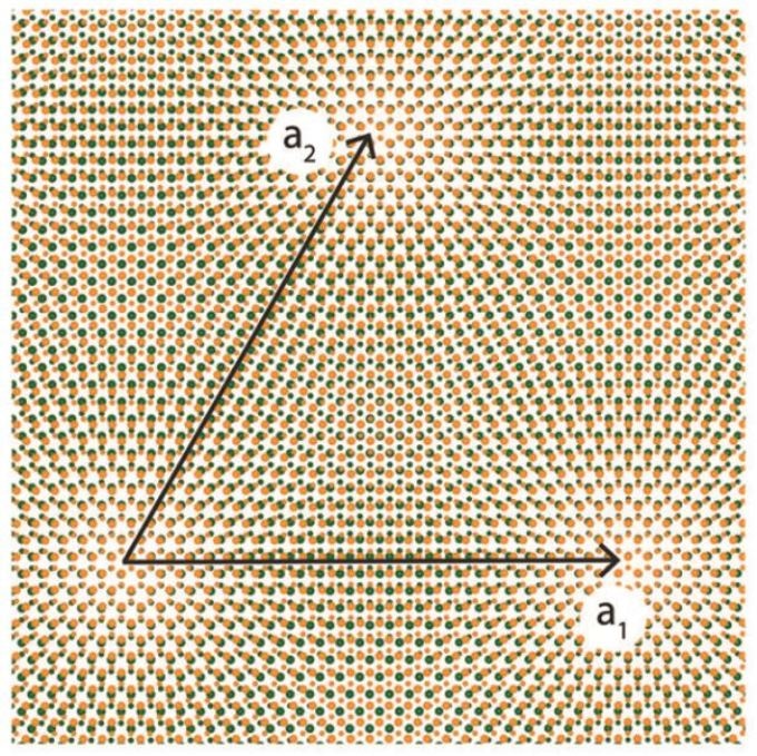
 The twist angle formed between atomically thin layers of tungsten disulfide and tungsten diselenide acts as a “tuning knob,” transforming these semiconductors into an exotic quantum material. (Image credit: Berkeley Lab)
Developments such as this could help to transform several industries having an eye for energy-efficient electronic systems, as well as offer a platform for exotic new physics.
The study explaining the technique, which involves stacking together 2D layers of tungsten diselenide and tungsten disulfide to develop an intricately patterned material, or superlattice, was reported recently online in the Nature journal.
“This is an amazing discovery because we didn’t think of these semiconducting materials as strongly interacting,” stated Feng Wang, a condensed matter physicist with Berkeley Lab’s Materials Sciences Division and professor of physics at UC Berkeley. “Now this work has brought these seemingly ordinary semiconductors into the quantum materials space.”
Two-dimensional (2D) materials, with a thickness of just one atom, are similar to nanosized building blocks that can be arbitrarily stacked to create tiny devices. A moiré superlattice, which is a repeating pattern, can be formed when the lattices of two 2D materials are well-aligned and similar.
Over the last 10 years, scientists have been investigating ways to integrate different 2D materials, usually beginning with graphene—a material familiar for its potential to efficiently conduct electricity and heat. Using these studies, other researchers had found that moiré superlattices created using graphene have exotic physics like superconductivity upon aligning the layers at just the right angle.
The new research, headed by Wang, involves using 2D samples of semiconducting materials, such as tungsten diselenide and tungsten disulfide, to demonstrate that the twist angle between layers offers a “tuning knob” to transform a 2D semiconducting system into an exotic quantum material that has highly interacting electrons.
Entering a New Realm of Physics
The tungsten diselenide and tungsten disulfide samples were fabricated by co-lead authors Chenhao Jin, a postdoctoral scholar, and Emma Regan, a graduate student researcher, both of whom work under Wang in the Ultrafast Nano-Optics Group at UC Berkeley. They achieved this by using a polymer-based method that involves picking up and transferring flakes of the materials, where the diameter of each flake is just tens of micrometers, into a stack.
For an earlier study, they had prepared similar samples of the materials but with both the layers stacked at no specific angle. They were totally astonished upon measuring the optical absorption of a new tungsten diselenide and tungsten disulfide sample for this study.
The absorption of visible light in a tungsten diselenide/tungsten disulfide device is the maximum when the light has the same energy as the exciton of the system. An exciton is a quasiparticle consisting of an electron attached to a hole, which is normal in 2D semiconductors. (In physics, a hole is a currently vacant state that can be occupied by an electron.)
The researchers expected to observe a single peak in the signal corresponding to the energy of an exciton, for light in the energy range that they considered.
Rather, they discovered that the original peak that they anticipated had split into three different peaks, that represented three distinct exciton states.
What could have led to the increase in the number of exciton states in the tungsten diselenide/tungsten disulfide device from one to three? Was it due to the moiré superlattice that was added?
In order to find answers to these question, their collaborators Aiming Yan and Alex Zettl used a transmission electron microscope (TEM) at Berkeley Lab’s Molecular Foundry, a nanoscale science research facility, to capture atomic-resolution images of the tungsten diselenide/tungsten disulfide device to examine how the lattices of the materials were aligned.
From the TEM images, what the researchers had suspected for a long time was confirmed: the materials had in fact formed a moiré superlattice.
We saw beautiful, repeating patterns over the entire sample. After comparing this experimental observation with a theoretical model, we found that the moiré pattern introduces a large potential energy periodically over the device and could therefore introduce exotic quantum phenomena.
Emma Regan, Graduate Student Researcher, Ultrafast Nano-Optics Group, UC Berkeley.
Next, the plan of the scientists is to evaluate how this new quantum system could be used in the field of optoelectronics, which involves using light in electronics; valleytronics, which involves extending the limits of Moore’s law by miniaturizing electronic components; and superconductivity, which would enables electrons to flow within devices with virtually no resistance.
Researchers from Arizona State University and the National Institute for Materials Science in Japan also contributed to the study.
The DOE Office of Science supported the study. Additional funding was offered by the National Science Foundation, the Department of Defense, and the Elemental Strategy Initiative conducted by MEXT, Japan, and JSPS KAKENHI. The Molecular Foundry is a DOE Office of Science user facility.