Feb 16 2018
Quantum dots have been making their mark in innovative and new applications and research advancements such as improved high-speed data transfer, LCD TVs, fluorescent labeling in biomedical applications, and thin-film solar cells.
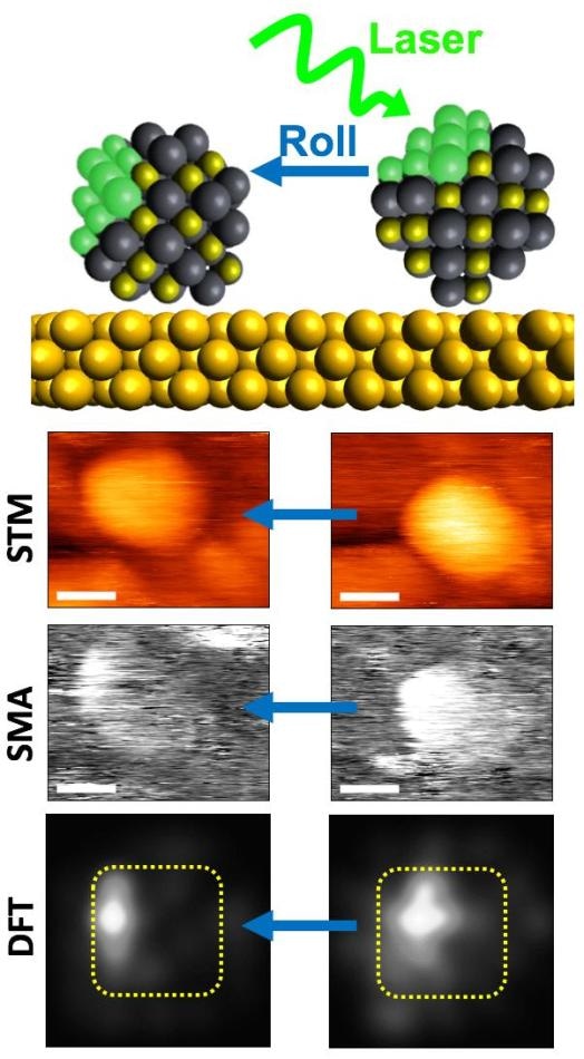
 Top: a Side-view image of a quantum dot with a defect excited by a laser (green) that rolled to present a different orientation. STM: Conventional STM image of a quantum dot before (right) and after a roll (left). SMA: a slice through the electronic density of the excited quantum dot before and after the same roll. DFT (density functional theory): 3-D quantum calculation of a quantum dot defect projected into slices at two orientations for comparison with experiment. (Image credit: Martin Gruebele)
Till date, scientists have been investigating the way to accurately regulate the growth of these nanoscale particles and their hidden quantum characteristic. For example, flaws are formed at the time of synthesizing semiconductor materials. Therefore, identical dots can vary in composition from each other.
In order to gain a more in-depth knowledge of these flaws, and whether they are beneficial or not, a team of U.S. researchers from the University of Illinois and the University of Washington has, for the first ever time, performed imaging of an electronically stimulated quantum dot at different orientations. Their results have been published in The Journal of Chemical Physics, from AIP Publishing.
Understanding how the presence of defects localizes excited electronic states of quantum dots will help to advance the engineering of these nanoparticles.
Martin Gruebele, Co-Author from the University of Illinois at Urbana-Champaign
Normally, flaws are regarded as a hindrance; however, for quantum dot applications, they are deliberately formed by doping the desired number of materials to provide particular functions.
[M]issing atoms in a quantum dot or substituting a different kind of atom are defects that will alter the electronic structure and change the semiconductivity, catalysis or other nanoparticle properties. If we can learn to characterize them better and precisely control how they are produced, defects will become desirable dopants instead of a nuisance.
Martin Gruebele, Co-Author from the University of Illinois at Urbana-Champaign
Gruebele’s group, in 2005, devised an innovative imaging method, known as single molecule absorption scanning tunneling microscopy (SMA-STM), which integrates the superior spatial resolution of a scanning tunneling microscope with a laser’s spectral resolution. SMA-STM enables imaging of individual nanoparticles in a laser beam, thus allowing visualization of their excited electronic structure.
Through the sharp, thin metal wire tip of the scanning tunneling microscope, they rotate the laser-stimulated quantum dot on the surface to image slices at disparate orientations. The slices can be integrated to reconstruct a 3-D image of an electronically stimulated quantum dot.
Although the study in this article was restricted to cadmium selenide/zinc sulfide and lead sulfide quantum dots, the method can be prospectively applied to other compositions. In addition, SMA-STM can also be applied to investigate other nanostructures, such as photocatalytic metal clusters and carbon nanotubes.
At present, scientists are striving to develop SMA-STM into a single-particle tomography method. However, prior to transforming SMA-STM into a “true single-particle tomography approach,” they have to make sure that the scanning and rolling do not damage the nanoparticle during its reorientation.
“We speculate that, in the future, it may be possible to do single-particle tomography if damage to quantum dots can be avoided during repeated manipulation,” stated Gruebele.
Single-particle tomography would offer a high-clarity picture when compared to traditional tomography by isolating flaws in individual nanoparticles instead of re-creating an averaged 3D image that integrates the evaluations of various particles.