Nov 29 2017
Highly efficient light sources are needed for tapping into the quantum properties of photons for optoelectronics. Lead trihalide perovskite nanocrystals display several properties that enable them to be promising candidates as light sources. Even though coupling quantum emitters with nanophotonic cavities can majorly enhance efficiency, this approach is yet to be explored with these nanocrystals.
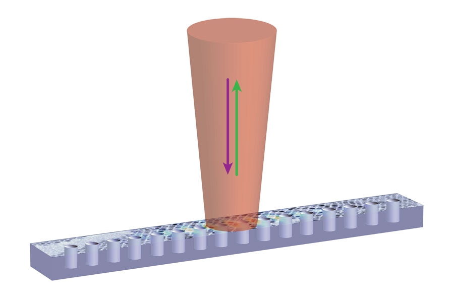
 The coupled device between the photonic crystal nanobeam cavity and perovskite nanocrystals, which overlays with the cavity mode profile. The arrows indicate that the excitation and generated signal are coupled in and out of the device vertically. CREDIT: Zhili Yang, University of Maryland
A group of researchers at the University of Maryland and ETH Zürich have recently demonstrated a simple approach used for coupling solution-synthesized cesium lead tribromide (CsPbBr3) perovskite nanocrystals to silicon nitride (SiN) photonic cavities. The subsequent room temperature light emission is improved by an order of magnitude above what perovskites can release alone. Doctoral candidate Zhili Yang and others have recently reported their results in Applied Physics Letters, from AIP Publishing.
Our work shows that it is possible to enhance the spontaneous emission of colloidal perovskite nanocrystals using a photonic cavity, our results provide a path toward compact on-chip light sources with reduced energy consumption and size.
Zhili Yang, Doctoral candidate, University of Maryland
The group drop cast perovskite nanocrystals in toluene solution onto the SiN cavity in order to couple the nanocrystals to the photonic cavity. This was then followed by exciting the device with a pulsed laser, causing photon emission from the nanocrystals.
The use of solutions to produce colloidal quantum emitters differs with the fabrication of epitaxial materials, an extensively used process that deals with growing crystalline overlayers on an existing substrate. Instead, Yang explained that, it is possible for one to directly deposit colloidal nanocrystals with the help of solvents more easily on a variety of wafers.
Similar perovskite materials are already considered to be promising in photovoltaic settings, and they also display several properties that make establish them to be promising candidates for light-emitting devices.
“The nanocrystals have a low density of defects that can trap carriers [electrons and holes], producing a very low nonradiative decay rate and a high photoluminescence efficiency at room temperature,” Yang said.
Attempts for emitting light with epitaxial materials have normally fallen short of competently covering the visible light spectrum, with the wavelength range in the blue-green being chiefly problematic. The device demonstrated by the team displayed emission centered at 510 nm in the green.
“The large challenge with this method, however, is that you have to find a very optimized concentration [density] of the crystals on the surface of the cavity,” Yang said. “It can’t be too condensed or else it will be detrimental to the cavity and might lead to nonconformity.”
The coupled nanocavity and nanocrystals boasted a tenfold improvement in emission brightness when compared to just the emitters alone. This resulted in a natural emission rate improvement of 2.9, which reflects an almost threefold increase in the photon emitting efficiency inside the cavity when compared to perovskites on unpatterned surfaces.
The results are a benefit to optoelectronics, Yang stated, a field that influences the quantum effects of photons on electronic materials in order to help build optical circuits that will not suffer from some of the inadequacies of purely electronic devices, such as heating. Optoelectronic devices are also capable of enjoying broader signal bandwidths and faster processing speeds, and could one day be employed in quantum communication networks and quantum computing.