Mar 3 2015
In the latest issue of the journal Nature Physics, German Scientists report that they could observe experimentally the current flow along channels at the crystal surfaces of topological insulators.
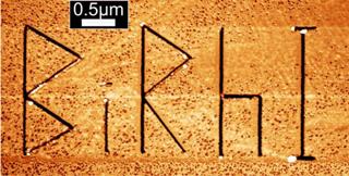
 Microscopic image of the topological insulator Bismuth-Rhodium-Iodine (Bi14Rh3I9). The engraved letters BiRhI act as artificially introduced steps at the crystal surface. Credit:M. Morgenstern, RWTH Aachen
The channels are less than one nanometer wide and extend along atomic steps of the crystal lattice. The scientists demonstrated also how these steps can be introduced in any arrangement.
Topological insulators are a hot topic in materials physics. The most prominent feature of these materials is that they act as both insulators and conductors, with their interior preventing the flow of electrical currents while their edges or surfaces allow the movement of charge.
German Scientist from RWTH Aachen, Research Center Jülich, TU Dresden and of the Leibniz Institute for Solid State and Materials Research Dresden report that the current flow on the surface of a topological insulator is channeled along tiny paths, which have been theoretically calculated and experimentally observed. Their work has been published in the issue from 2 March 2015 of the journal Nature Physics. There they show for Bismuth-Rhodium-Iodine that these channels are tied to one dimensional surface features and run along steps formed by the edges of atomic layers. Scanning tunneling spectroscopy reveals the electron channels to be continuous in both energy and space and less than one nanometer wide.
Due to the properties of topological insulators, electric current flows unimpeded within these channels while charge can barely move from one channel to another. In this way, the surface acts as a set of electric wires that is defined by the atomic steps at the crystals surface. The scientists demonstrated that the surface can be engraved in any arrangement, allowing channel networks to be patterned with nanometer precision. The channeled current flow enables the transport of electrons while preventing the "scattering" typically associated with power consumption, in which electrons deviate from their trajectory. Thus, the resulting energy losses and heat generation are substantially diminished. These properties make topological insulators interesting for application in electronics. Furthermore, they are expected to enable novel types of information processing such as spintronics or quantum computation. However, the prerequisite for the development of new devices based on topological insulators is a profound understanding of these quantum phenomena. The recent publication marks a milestone in this direction.
During the last decade great effort are being made worldwide to investigate and to describe the transport in topological insulators. In 2013 the team of Professor Michael Ruck at TU Dresden has succeeded for the first time in growing single crystals of Bismuth-Rhodium-Iodine. Jointly with theoreticians from the Leibniz-Institute for Solid State and Materials Research Dresden they concluded that these crystals are topological insulators with electrical conducting channels. The recent experiments at RWTH Aachen and combined calculations in Dresden have now proved this hypothesis.