Dec 17 2012
A new material structure predicted at Rice University offers the tantalizing possibility of a signal path smaller than the nanowires for advanced electronics now under development at Rice and elsewhere.
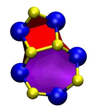
 An animated illustration shows the precise arrangement of atoms in one possible dislocation in two-dimensional molybdenum/sulfur. Dislocations happen when two growing blooms of material come together at different angles in chemical vapor deposition. (Credit: Xiaolong Zou/Rice University)
Theoretical physicist Boris Yakobson and postdoctoral fellow Xiaolong Zou were investigating the atomic-scale properties of two-dimensional materials when they found to their surprise that a particular formation, a grain boundary in metal disulfides, creates a metallic – and therefore conducting – path only a fraction of a nanometer wide.
That's basically the width of a chain of atoms, Yakobson said.
The discovery reported this week in the American Chemical Society journal Nano Letters sprang from an investigation of how atoms energetically relate to each other and form topological defects in two-dimensional semiconductors. In recent work, Yakobson's group has analyzed defects in graphene, the single-atom sheet of carbon that is under intense scrutiny by labs around the world.
But flat graphene has no band gap; electrons flow straight through. "There is a lot of effort to open a gap in graphene, but this is not easy," said Yakobson, Rice's Karl F. Hasselmann Professor of Mechanical Engineering and Materials Science and professor of chemistry. "People are trying different ways, but none of them are straightforward. This motivated the search for other two-dimensional materials."
Molybdenum/sulfur (or tungsten/sulfur) materials are becoming interesting to scientists because they have a useful natural band gap, about two electron volts in the case of molybdenum/sulfur. And while they are technically two-dimensional materials, the energies at play force their atoms into a staggered arrangement.
"It's more complex than graphene," Yakobson said. "There's a layer of metal in the middle, with sulfur atoms above and below, but they're fully connected by covalent bonds in a honeycomb lattice, so it's one compound."
Chemical vapor deposition is typically used to grow such material; under high temperatures the atoms (like carbon for graphene) fall into line and form sheets. But when two such blooms appear and they meet, they don't necessarily line up. Where they merge, they form what are called "grain boundaries," akin to grains in wood that join at awkward angles. (Think of a branch meeting a tree trunk.) Those grain boundaries affect the electrical properties of the merged material.
Zou calculated those properties based on the atomic energies of the elements. In looking at the elemental bonds, the researchers found the expected "dislocations" where the energies force atoms out of their regular patterns. "Where the sheets meet, they cannot have an ideal lattice structure, so they have these stitches, the dislocations. Each grain boundary is just a series of these dislocations," Yakobson said.
It was only coincidence that the dislocations took on dreidel-like shapes for a paper published during Hanukkah, he said.
"We found order in this complexity and chaos, the exact structures that are possible at the grain boundaries and the dislocations types," he said.
The growing molybdenum/sulfur sheets can meet at any angle, and though the sheets are semiconducting, the boundaries between them generally stop electrical signals in their tracks. But at one particular angle -- 60 degrees -- the periodic dislocations are close enough to pass signals on from one to the next along the length of the boundary. "Basically, they're metallic in this direction," Yakobson said.
"So in the middle of these domains of semiconducting material, you have this boundary line that carries current in one direction, like a wire. And it's only a few angstroms wide," he said.
"Metal disulfides may be promising for future electronic devices based on materials with reduced dimensions," Zou said. "It is important to understand the effects of topological defects on the electronic properties as we push toward post-silicon devices."