Mar 19 2014
Saroj Prasad Dash, Assistant Professor in microtechnology and nanoscience at Chalmers University's Quantum Device Physics Laboratory explains his research and thoughts on electron and spin transport in nanodevices.
Please, give us a description of your current research?
The research focus of our group at Chalmers is on “spintronic devices”, using semiconductor nanostructures, graphene, and other two-dimensional (2D) layered materials. We explore designer heterostructures of 2D layered materials for next generation spintronics devices.
By stacking various 2D atomic crystals on top of each other, we aim to create van der Waals heterostructures which hold promise for novel devices with designed spintronic properties. In addition, new fundamental physics not present or accessed in individual 2D crystals is widely expected to emerge in their van der Waals heterostructures. The goal is to exploit spin degree of freedom of electrons for integration of memory and logic functionalities in nanoelectronic devices.
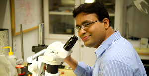
 Saroj Prasad Das. Photo: Peter Widing
This could for instance allow a new high-performance generation of computing that required far less power than conventional computing. Spin-based technologies may have a further profound impact on nanoelectronics, data storage, and logic and computer architectures
What are the latest developments in your area?
In recent years, devices utilizing electron spin functionalities has been demonstrated on several semiconductors and graphene. Our group and several other groups have shown that it is possible to generate and detect spin polarization in semiconductors and graphene at room temperature using conventional ferromagnetic tunnel contacts. However, such structures are prone to degraded device performance with low spin polarization and lifetime in these materials, and therefore many of the interesting spin functionalities could not be accessed. Also most of these 2D materials are very recently discovered; therefore giving lots of opportunities to explore their unique spin related properties.
Which future challenges do you find most exciting?
The “holy grail” of spintronics research is “spin injection, transport and manipulation” in 2D layered materials. 2D library provides large class of interesting materials for spintronics: conducting graphene for its long spin coherence length, semiconducting transition metal di-chalcognides with high spin orbit coupling for spin-manipulation, insulating hexagonal boron nitride tunnel barrier for spin polarized tunneling, and topological insulators for spin polarized surface states. In addition, to interesting spin physics present in these individual 2D crystals, the challenging goal is to discover new fundamental physics widely expected to emerge when we stack various 2D atomic crystals on top of each other, in their van der Waals heterostructures.
In which way, could your research benefit society at large?
Spintronics research offers new knowledge about generation and control of spin degree of freedom of electrons in nano devices of semiconductors, 2D materials, and their heterostructures. The International Technology Roadmap for Semiconductors has also identified spin as an alternative state viable for future nanoelectronic device applications. In addition to the near-term studies of various spin based logic and memory devices, a long-term and ambitious goal of spintronics research is the application of electron spins to quantum information processing and quantum computation.