Mar 4 2014
In physics, there's small, and then there's nullity – as in zero-dimensional.
University of Cincinnati researchers have reached this threshold with a special structure that may someday lead to better ways of harnessing solar energy, stronger lasers or more sensitive medical diagnostic devices.
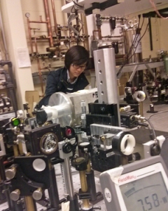
 UC student Teng Shi will present her semiconductor nanowire research at the American Physical Society meeting.
These structures are semiconductor nanowires. UC doctoral student Teng Shi says she and a team of researchers have observed unique optical signatures indicating that electronic excitations within these nanowires can be confined to a zero-dimensional state called a "quantum dot."
This latest discovery is all about going small, but its significance is anything but. The research team’s ability to control the confinement energy by varying the size of the quantum dot opens up a world of possibilities.
"Exploring the basic physics of semiconductor nanowires enables one to envision applications or to design structures for applications," says Shi of UC's Department of Physics. "These structures are potential candidates for a variety of applications including photovoltaics, lasers and ultra-sensitive nanosensors."
Shi will present the team's research "Temperature-dependent Photoluminescence Imaging of GaAs/AlGaAs Heterostructure Quantum Well Tubes" at the American Physical Society (APS) meeting to be held March 3-7 in Denver. Nearly 10,000 professionals, scholars and students will attend the APS meeting to discuss new research from industry, universities and laboratories from around the world.
This research advances work previously done on semiconductor nanowires at UC. By using a thin shell called a quantum well tube and growing it – to about 4 nanometers thick – around the nanowire core, researchers found electrons within the nanowire were distributed in an unusual way in relation to the facets of the hexagonal tube. The result is a quantum wire, like a long string many times thinner than a human hair.
Now they've taken things even further, going from one-dimensional wires to zero-dimensional quantum dots. These little structures could have a big effect on a variety of technologies. Semiconductors are at the center of modern electronics. Computers, TVs and cellphones have them. They’re made from the crystalline form of elements that have scientifically beneficial electrical conductivity properties. Many semiconductors are made of silicon, but gallium arsenide is used in this research.
Additional contributors to this research are UC physics professors Howard Jackson and Leigh Smith in the McMicken College of Arts and Sciences; Jan Yarrison-Rice of Miami University; and Nian Jiang, Hoe Tan, Qiang Gao and Chennupati Jagadish of Australian National University.
The team at UC is one of only about a half dozen in the U.S. conducting competitive research in the field, and UC’s efforts in this area are partially funded by the National Science Foundation. The team's big achievements in the science of small support the UC2019 Academic Master Plan by producing new ways of understanding and transforming the world through research and scholarship.